Key Processes in Semiconductor Manufacturing
Understanding Key Processes in Semiconductor Manufacturing
Semiconductor manufacturing is a marvel of precision engineering, involving a series of highly specialized processes to create microchips that power modern technology. Among these, photolithography, deposition, and etching are foundational steps. Each plays a vital role in defining the intricate features of semiconductor devices, ensuring functionality and performance at nanometer scales. Let’s explore these processes in detail and understand why maintaining precision is paramount.
Photolithography: Defining Patterns
Photolithography is the cornerstone of semiconductor manufacturing, enabling the transfer of intricate patterns from a photomask onto a silicon wafer. This process involves several key steps:
- Coating the Wafer: A light-sensitive material called photoresist is applied to the wafer's surface.
- Exposure: Ultraviolet (UV) light shines through a photomask, projecting the mask's pattern onto the photoresist.
- Development: The exposed photoresist is chemically developed, leaving behind a precise pattern.
Purpose: Photolithography defines the micro-scale features and circuit layouts that form the blueprint of a semiconductor chip. This precision step ensures that transistors, interconnects, and other components are correctly positioned and sized.
Deposition: Building Layers
Deposition is the process of adding thin layers of materials—such as metals, insulators, or semiconductors—onto the wafer’s surface. These layers are critical for creating structures that allow a chip to function. There are two main deposition methods:
- Physical Vapor Deposition (PVD): Material is vaporized in a vacuum chamber and condensed onto the wafer to form a thin film.
- Chemical Vapor Deposition (CVD): Chemical reactions are used to deposit a thin layer of material from gaseous precursors.
Purpose: Deposition builds the conductive pathways, insulating barriers, and other essential layers that enable the chip to perform complex operations. Each layer must be uniformly deposited to ensure reliability and performance.
Etching: Creating Features
Etching is a subtractive process used to remove specific parts of the material deposited on the wafer, creating the desired patterns and structures. It typically follows photolithography to refine the circuit patterns. There are two primary etching methods:
- Wet Etching: Uses liquid chemicals to dissolve unwanted material.
- Dry Etching (Plasma Etching): Employs reactive gases or plasma to achieve precise removal at a microscopic level.
Purpose: Etching carves out intricate features such as trenches, contact holes, and circuit pathways, essential for the chip's electrical functionality.
The Importance of Precision
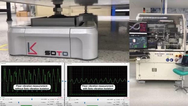
Each of these processes operates at nanometer scales, where even the slightest disturbance can cause defects. Vibrations, temperature fluctuations, or environmental inconsistencies can disrupt the delicate alignment and accuracy required in photolithography, deposition, etching. These defects can lead to reduced yields and compromised chip performance.
How KNS Leads in Overcoming Manufacturing Challenges
This is where KNS Advanced Systems Ltd. steps in. Founded with a mission to tackle the most demanding challenges of precision engineering, KNS has developed state-of-the-art vibration isolation and environmental control technologies. These solutions are specifically designed to address the needs of semiconductor manufacturers.
By integrating advanced vibration control systems, KNS ensures a stable manufacturing environment, minimizing risks such as misalignment and defects. Their cutting-edge innovations have become a critical component in maintaining the precision necessary for processes like photolithography, deposition, etching.
The company’s slogan, "Nonstop Innovating," reflects its commitment to pushing the boundaries of what’s possible in semiconductor manufacturing. With a relentless focus on research and development, KNS empowers manufacturers to achieve higher yields, improved chip performance, and reduced operational risks.
Photolithography, deposition, and etching are the backbone of semiconductor manufacturing, transforming silicon wafers into the microchips that drive modern innovation. Each process requires extreme precision, and maintaining stability during these steps is critical for ensuring high yields and superior performance.
With the groundbreaking technologies developed by K&S Advanced Systems Ltd., manufacturers can overcome environmental disturbances, ensuring that every microchip meets the exacting standards of today’s tech-driven world. Investing in solutions from leaders like KNS is not just an enhancement—it is an essential component of modern manufacturing excellence.


